
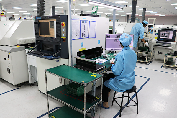
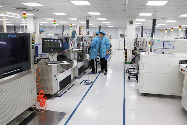
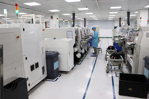
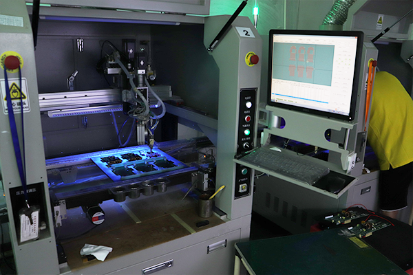
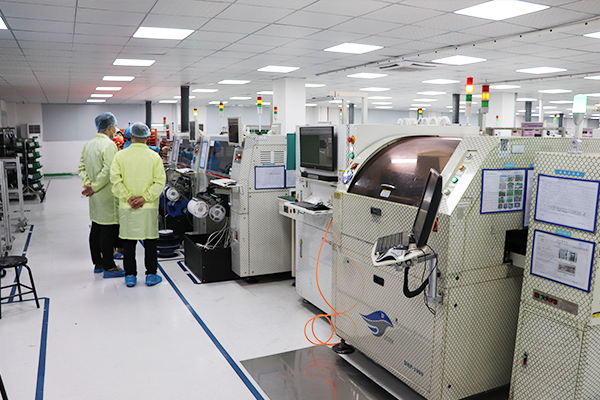
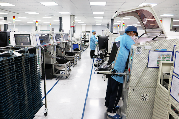
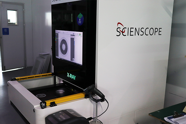
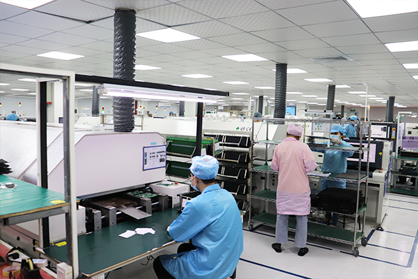
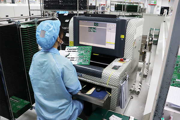
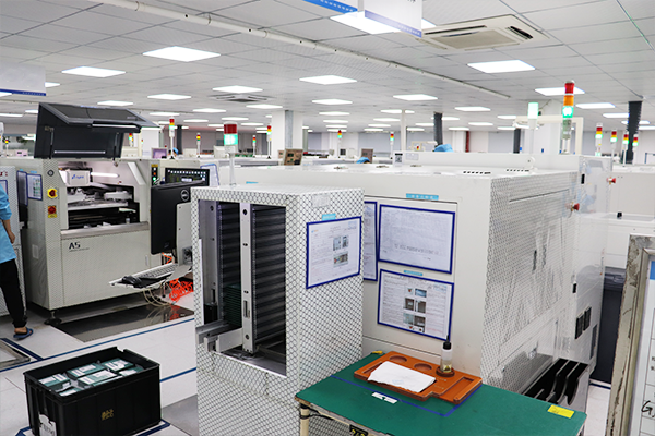
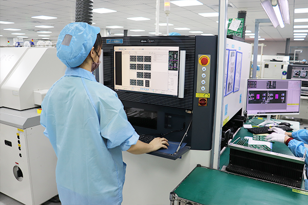
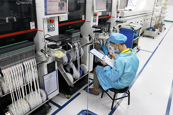
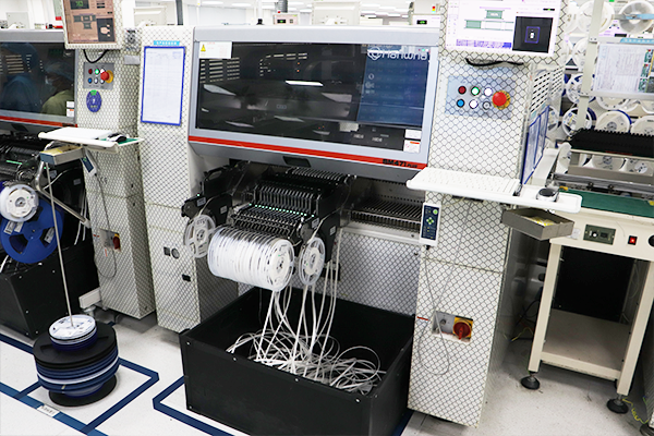
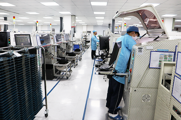
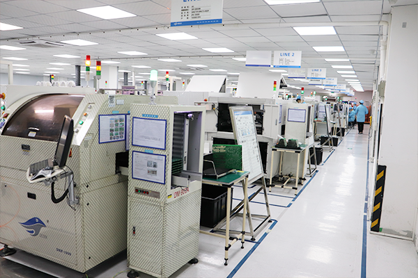
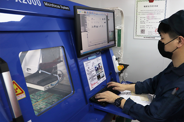
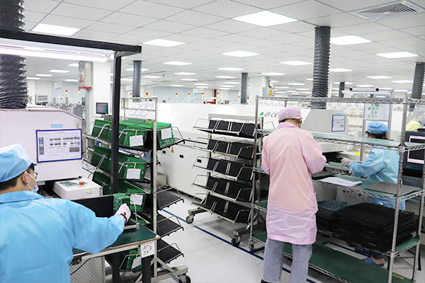
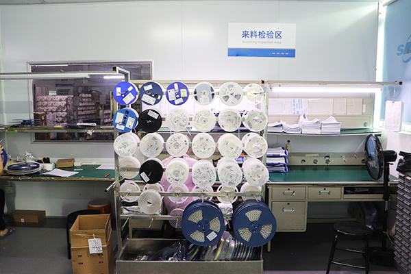
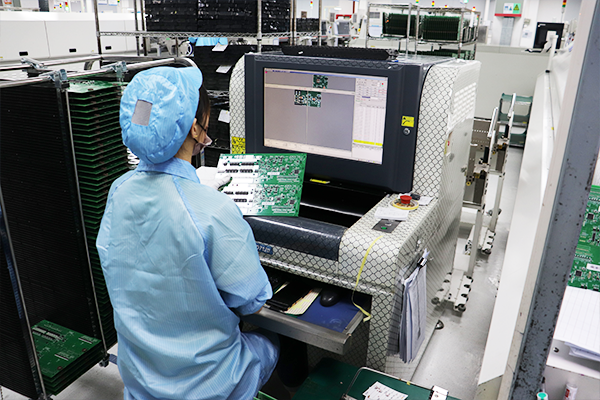
We operate 6 dual-track placement lines equipped with imported Yamaha YSM20 and Samsung placement machines, fully automatic solder paste printers, AOI (Automatic Optical Inspection), X-Ray, and SPI (Solder Paste Inspection), along with other state-of-the-art equipment. We boast a daily mounting capacity of 3 million solder joints, with specialized expertise in high-precision and complex single-board assembly—and a proven track record in manufacturing ultra-complex single boards exceeding 10,000 solder joints.
| SMT Lines | 6 Double Track Automatic Lines |
| SMT Daily Capacity | 3,000,000 Solder Joints |
| DIP Lines | 2 Semi-Automatic Lines |
| DIP Daily Capacity | 200,000 Solder Joints |
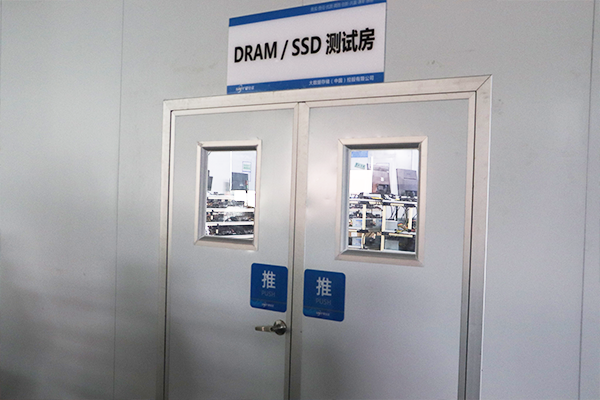
| Test Lines | 2 Semi-Automatic Lines |
| Solder Paste Thickness Detection | 2D + 3D SPI |
| AOI Inspection | 2D + 3D AOI |
| Defect Rate | 0.3% for Resistors/Capacitors |
| Zero IC Component Loss | |
| Conformal Coating Thickness | 3-15μm |
| Mountable Component Specifications | Minimum Component Package | 1005 |
| Minimum Component Accuracy | ±0.04mm | |
| Pin/BGA Pitch | Chip/0.35 Pitch BGA | |
| IC SMT Placement Accuracy | ±0.04mm | |
| Maximum Component Weight | 150g | |
| Maximum Component Size | 150mm*150mm | |
| Maximum Component Height | 25mm | |
| Compatible PCB Specifications | PCB Size | 50*50mm - 650*500mm |
| PCB Thickness | 0.3-6.5mm | |
| PCB Types | Splicing Board/Veneer | POP/Regular Board/FPC/Rigid Flex Bonding Board/Metal Substrate |


| Specification | Prototype | |
|---|---|---|
| Number Of Layers | 2-48 L | 2-36 L |
| Board Thickness | 0.2-17.5mm | 0.2-10mm |
| Minimum Mechanical Aperture | 0.15mm | 0.15mm |
| Minimum Laser Aperture | 3mil | 4mil |
| HDI Type | 1+n+1,2+n+2,······,Anylayer (Any layer interconnection) | 1+n+1,2+n+2,······,Anylayer (Any layer interconnection) |
| Minimum Line Width&Spacing | 2/2mil | 3/3mil |
| Impedance Control | +/-5% | +/-10% |
| Maximum Copper Thickness | 12oz | 6oz |
| Maximum Plate Thickness Aperture Ratio | 18:1 | 16:1 |
| Maximum Board Size | 650mm X 1130mm | 610mm X 1100mm |
| Board Material | FR4/Hi-Tg/Rogers/Halogen Free/ RCC/PTFE/Nelco/Mixed Pressure Material |
|
| Surface Treatment | HASL、HASL PB FREE Immersion Gold/Tin/Silver Gold Finger Plating OSP、Immersion Gold + OSP |
|
| Special Processes | Buried/blind holes, step grooves, metal substrates, buried resistors, buried capacitors, mixed voltage, rigid-flex bonding, back drilling, step gold fingers, etc. | |
| Number Of Layers | Mass Production | Prototype | Urgent Order |
|---|---|---|---|
| 2 layers | 9 days | 5 days | 48 Hours |
| 4 layers | 10 days | 5 days | 3 days |
| 6 layers | 12 days | 6 days | 3 days |
| 8 layers | 12 days | 7 days | 4 days |
| 10 layers | 14 days | 10 days | 4 days |
| 12 layers | 16 days | 10 days | 5 days |
| 14 layers | 18 days | 12 days | 6 days |
| 16 layers | 18 days | 12 days | 6 days |
| 18 layers | 20 days | 14 days | 6 days |
| 20 layers | 20 days | 14 days | 10 days |
| 22 layers | 22 days | 14 days | 10 days |
| 24 layers | 24 days | 14 days | 10 days |
| 26 layers | 26 days | 14 days | 10 days |
| 28 layers | 28 days | 14 days | 10 days |
| 30 layers | 30 days | 14 days | 10 days |
| 32 layers | 32 days | 14 days | 10 days |
Note: Delivery times exclude engineering lead time (typically 2-7 days). Contact our team for customized delivery schedules.
1500+Users Choose Gaode Electronics, Pcb Board Processing And Manufacturing, One-Stop Service, Gaode Electronics Helps Enterprises Develop Rapidly
Business Hours: Monday to Saturday:08:00-22:00
Email:sales@aceodm.com
Fax:0755-29194291
 Customer Service
Customer Service
Customer Service